
More project photos (2)
The problem
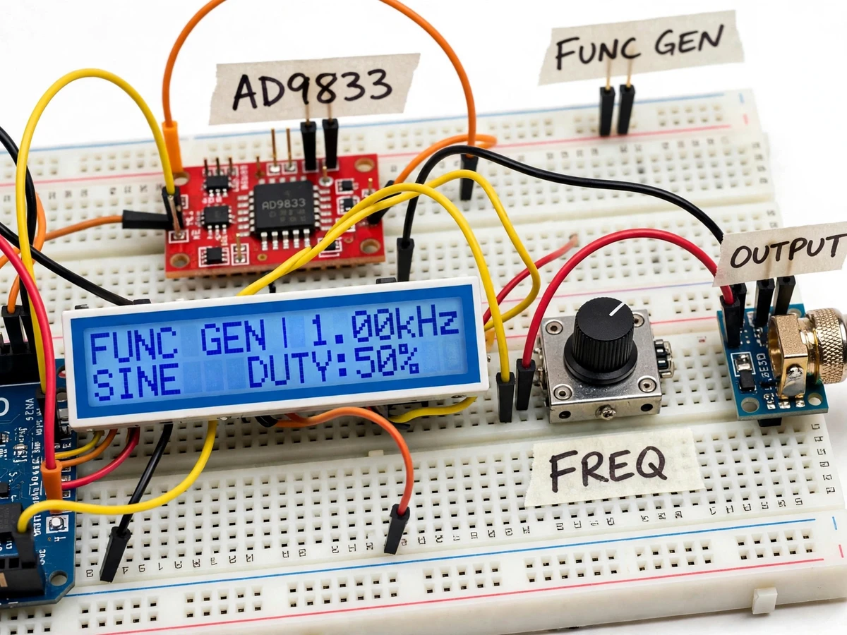
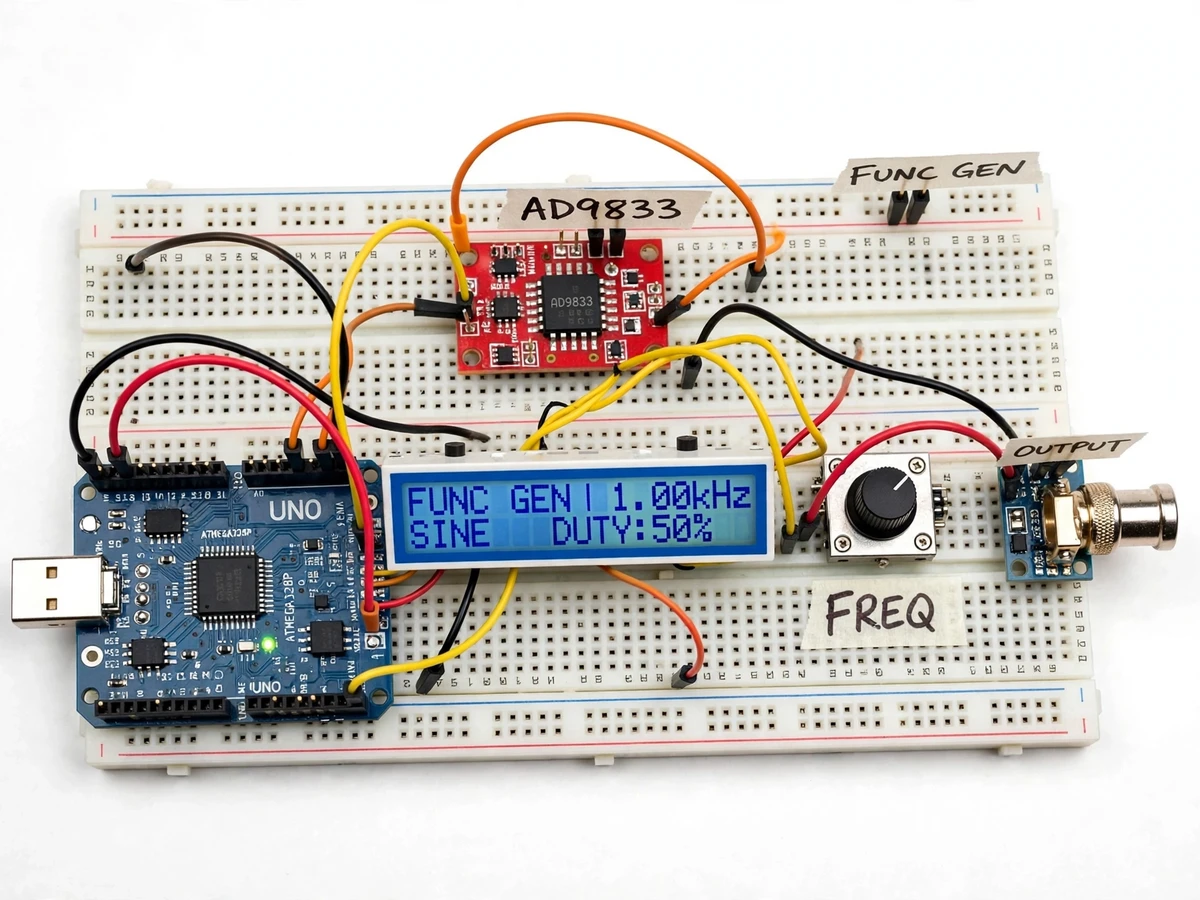
A function generator is one of the most-used instruments in an electronics lab, but students rarely get hands-on time with one — shared benches mean long queues before a practical, and affordable bench instruments are far outside a student budget. Meanwhile, the typical DIY "signal generator" project is just an Arduino PWM pin with a filter, topping out at audio frequencies with visibly distorted output. The useful middle ground is a real direct digital synthesis chip: the AD9833 is a genuine waveform-generator IC that produces sine, triangle and square waves with datasheet-rated performance up to 12.5 MHz, and it speaks SPI — so an Arduino can program it like a real instrument. This project builds exactly that: an AD9833 DDS module programmed by an Arduino Uno, with a rotary encoder for frequency and waveform selection, a 16x2 LCD showing the live settings, and a BNC output connector ready for the CRO probe.
Knob that steps frequency up or down; the push action switches the digit step or the waveform type.
Follow the working sequence
How it works
- The Arduino powers up and initializes the AD9833 over SPI: reset bit, then the control register selects waveform mode and enables output.
- The target frequency is converted to the AD9833's 28-bit frequency word (frequency word = desired Hz × 2^28 / 25 MHz MCLK) and written to the selected frequency register pair.
- Turning the rotary encoder increments or decrements the frequency by the current step size; pressing it moves the step digit or switches waveform.
- Each change rewrites the frequency and control registers over SPI; the LCD is refreshed to show the new frequency and waveform name.
- The AD9833's phase accumulator advances at the 25 MHz master clock, its lookup table produces the waveform samples, and the on-chip 10-bit DAC outputs the analog wave.
- The module's onboard filter and buffer stage conditions the output, which appears at the BNC jack for measurement or CRO display.
- During review, the student verifies the output on a lab oscilloscope and records measured frequency and waveform screenshots for the report.
Tech stack:
- Arduino Uno (ATmega328P, 3-wire SPI master)
- AD9833 DDS waveform-generator IC (28-bit frequency registers)
- Embedded C firmware (Arduino IDE)
- 16x2 character LCD with I2C backpack
- Rotary encoder (frequency/waveform control)
- Solderless breadboard + jumper-wire construction
- BNC output jack for CRO/DSO connection
- Lab oscilloscope + frequency counter (verification)
| Parameter | Value |
|---|---|
| Waveform types | Sine, triangle, square (AD9833 datasheet wave types) |
| Frequency range | 0.1 Hz to 12.5 MHz (datasheet, 25 MHz MCLK on the module) |
| Frequency tuning resolution | Approximately 0.093 Hz (25 MHz / 2^28, datasheet-derived) |
| Output level | DAC-native, approximately 0.6 Vpp typical (no amplifier stage in base build) |
| Control interface | 3-wire SPI from Arduino, control + frequency registers |
| User interface | Rotary encoder + push-select, 16x2 character LCD |
| Supply | 5 V (Arduino USB or adapter); AD9833 rated 2.3–5.5 V per datasheet |
| Output connector | Panel BNC jack, high-impedance load recommended |
| Build form | Solderless breadboard prototype, labeled modules |
Project features
- [Real AD9833 DDS waveform core] A genuine AD9833 direct digital synthesis IC (28-bit frequency registers) generates sine, triangle and square waves — a real instrument-grade waveform source, not filtered PWM.
- [Rotary-encoder control] Turn the knob to dial frequency up and down; the encoder also switches waveform type and digit-step selection, giving an instrument-like feel.
- [Live 16x2 LCD readout] The display continuously shows the set frequency and selected waveform, so the settings are always visible during a demo.
- [SPI register programming] The Arduino writes the AD9833 control and frequency registers over 3-wire SPI, and the report explains the register map for the viva.
- [BNC output connector] The module output is routed to a panel BNC jack, so the student can plug straight into a CRO or DSO for live waveform demos.
- [Breadboard prototype build] Built on a solderless breadboard with labeled modules and jumper wiring — easy to show, explain and debug in a review.
- [Buyer-run verification procedure] A step-by-step procedure to verify frequency and waveform shape on a lab oscilloscope/frequency counter, with readings the student records themselves.
What is included
- Working breadboard prototype: Arduino Uno, AD9833 DDS module, 16x2 LCD, rotary encoder, BNC output
- Arduino firmware with documented SPI register writes and encoder/LCD handling
- Wiring diagram and connection table (module pins to Arduino pins)
- Buyer-run verification procedure for oscilloscope and frequency-counter checks
- Project report PDF (DDS theory, AD9833 register map, methodology, verification results)
- PPT presentation for final review
- Viva Q&A preparation document (DDS vs PWM, SPI protocol, frequency-word math, waveform generation)
Limitations & prerequisites
- The 12.5 MHz ceiling is the AD9833 datasheet Nyquist limit with the module's 25 MHz crystal; sine shape is cleanest below a few MHz and degrades near the top of the band.
- The base build has no power-amplifier stage: the ~0.6 Vpp DAC-level output suits high-impedance loads (CRO, buffer input); driving 50 Ω loads or speakers needs an optional op-amp output stage.
- This is a student prototype, not a calibrated instrument: output accuracy is a design target bounded by the 25 MHz crystal's tolerance, and the report records the student's own oscilloscope-verified readings, not factory calibration.
- The 16x2 LCD shows two short rows, so frequency and waveform are displayed compactly; no graphical waveform preview is possible on the character display.
- Breadboard construction keeps assembly demo-friendly, but long jumper leads pick up noise at higher frequencies — the build targets lab-demonstration quality, not metrology-grade signal purity.
- Rotary-encoder steps are firmware-defined; the finest practical step is limited by the encoder detents and the debounce handling, not the 0.093 Hz DDS resolution.
Frequently Asked Questions
How is this different from an Arduino PWM "signal generator"?
PWM projects filter a digital pin and realistically top out in the audio band with visible distortion. The AD9833 is a genuine direct digital synthesis IC: a phase accumulator, sine lookup table and 10-bit DAC inside one chip, datasheet-rated to 12.5 MHz with true sine, triangle and square outputs.
What does the Arduino actually do?
The Arduino is the instrument controller. It computes the 28-bit frequency word for the desired frequency, programs the AD9833 control and frequency registers over SPI, reads the rotary encoder for user input, and drives the LCD that shows frequency and waveform.
Can I see the output on a CRO?
Yes — that is the intended demo. The output goes to a BNC jack; connect a CRO/DSO probe and you see the live sine, triangle or square wave. The verification procedure walks through recording frequency and capturing waveform screenshots for the report.
How accurate is the frequency?
Frequency accuracy is a design target bounded by the 25 MHz master-clock crystal's tolerance, and tuning resolution is approximately 0.093 Hz from the 28-bit register math. The build includes a procedure to check the output against a lab frequency counter, and the report carries the student's own measured figures.
Can it drive a speaker or a 50 Ω load?
Not in the base build — the ~0.6 Vpp DAC-level output is meant for high-impedance inputs like a CRO or a buffer. Driving heavier loads needs an op-amp output stage, which is documented as an optional extension.
Is this project suitable for a final-year project?
Yes — for Electronics, E&TC and IoT & Embedded programs. It combines a real mixed-signal IC, SPI register-level programming, encoder/LCD user interfacing and instrument-style verification on a CRO. Suitable for B.E./B.Tech final-year projects in Electronics, Electronics & Telecommunication and IoT & Embedded.
Components & software requirements
- Arduino Uno (ATmega328P, 3-wire SPI master)
- AD9833 DDS waveform-generator IC (28-bit frequency registers)
- Embedded C firmware (Arduino IDE)
- 16x2 character LCD with I2C backpack
- Rotary encoder (frequency/waveform control)
- Solderless breadboard + jumper-wire construction
- BNC output jack for CRO/DSO connection
- Lab oscilloscope + frequency counter (verification)
Delivery information
Built-to-order project. Delivery timeline is shared after order confirmation based on current queue.
Support terms
Complete documentation, setup guide, and viva preparation included. Support for setup and explanation provided.
Download free synopsis (PDF)
Enter your name and email — the synopsis PDF downloads immediately. We may send occasional project updates; no spam, unsubscribe anytime.