
More project photos (3)
The problem
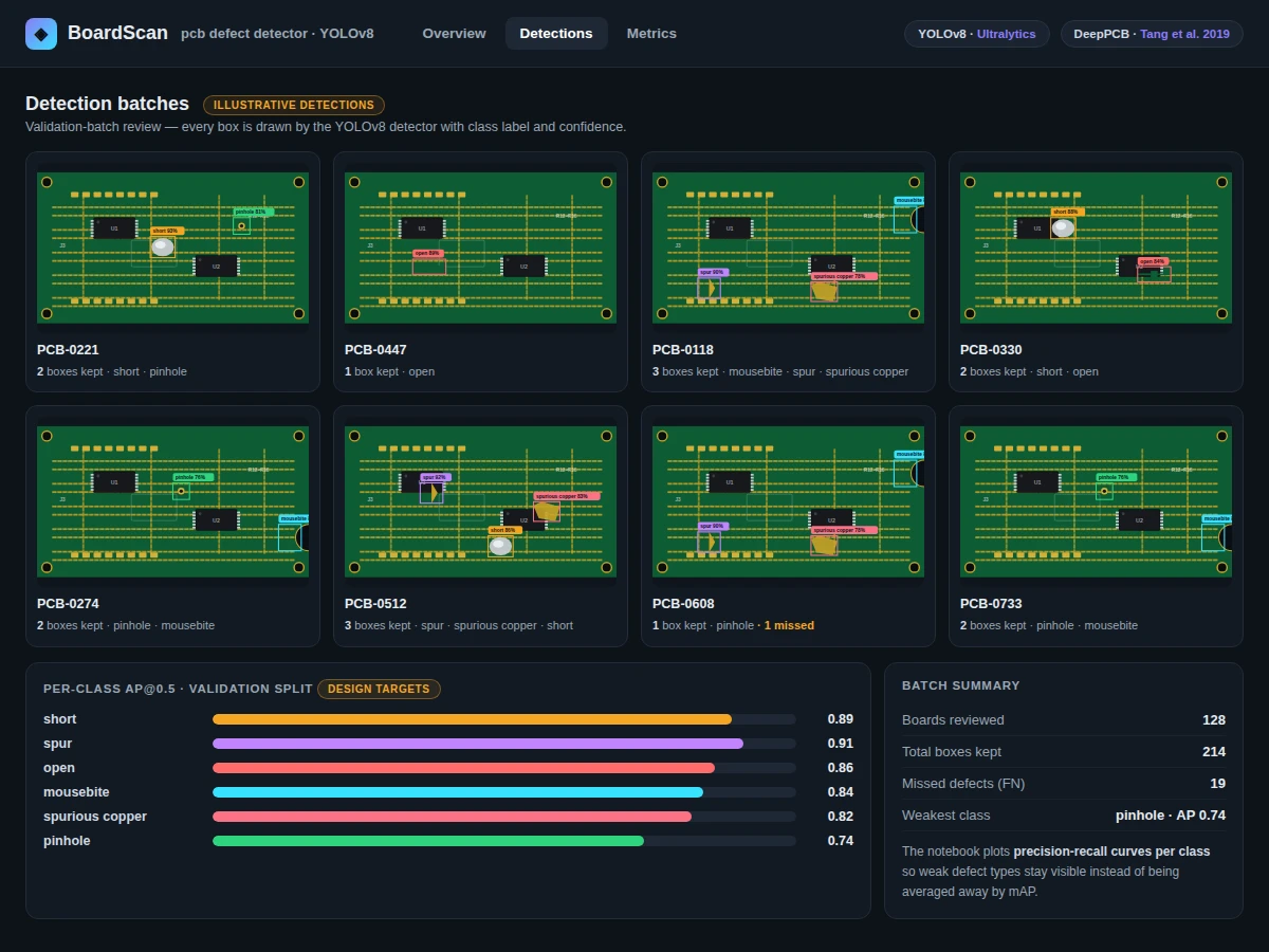
Printed circuit boards are inspected for soldering and component defects — opens, shorts, mousebites, spurs, pinholes and spurious copper — that manual visual inspection misses on dense, fast-moving lines. A classifier can only say whether a board image contains a defect; an inspector needs to know where each defect is and what kind it is. Object detection answers both: a YOLO detector predicts where each defect is, drawing a bounding box with a class label and confidence score in a single pass. The difficulty is localizing small, varied defects against complex board backgrounds — copper pours, silkscreen and solder texture all look deceptively defect-like. This project studies the idea end to end, training YOLOv8 on the public DeepPCB dataset (Tang et al. 2019) with its six defect types, and evaluating detection quality with per-class metrics so weak defect types are not hidden behind an average — including a visualization script so every prediction can be verified by eye.
Uploads PCB images for defect scanning.
Follow the working sequence
How it works
Dataset & model:
Dataset name: DeepPCB (Tang et al., "Online PCB defect detector on a new model of PCB defect dataset", arXiv:1902.06197, 2019).
Source: Official academic release of the DeepPCB dataset.
Task: Object detection (defect localization with bounding boxes).
Classes: Six defect types — open, short, mousebite, spur, pinhole, spurious copper — per the official dataset documentation.
Model: YOLOv8 (Ultralytics) single-pass detector, pre-trained on COCO and fine-tuned on DeepPCB; PyTorch as the training backend.
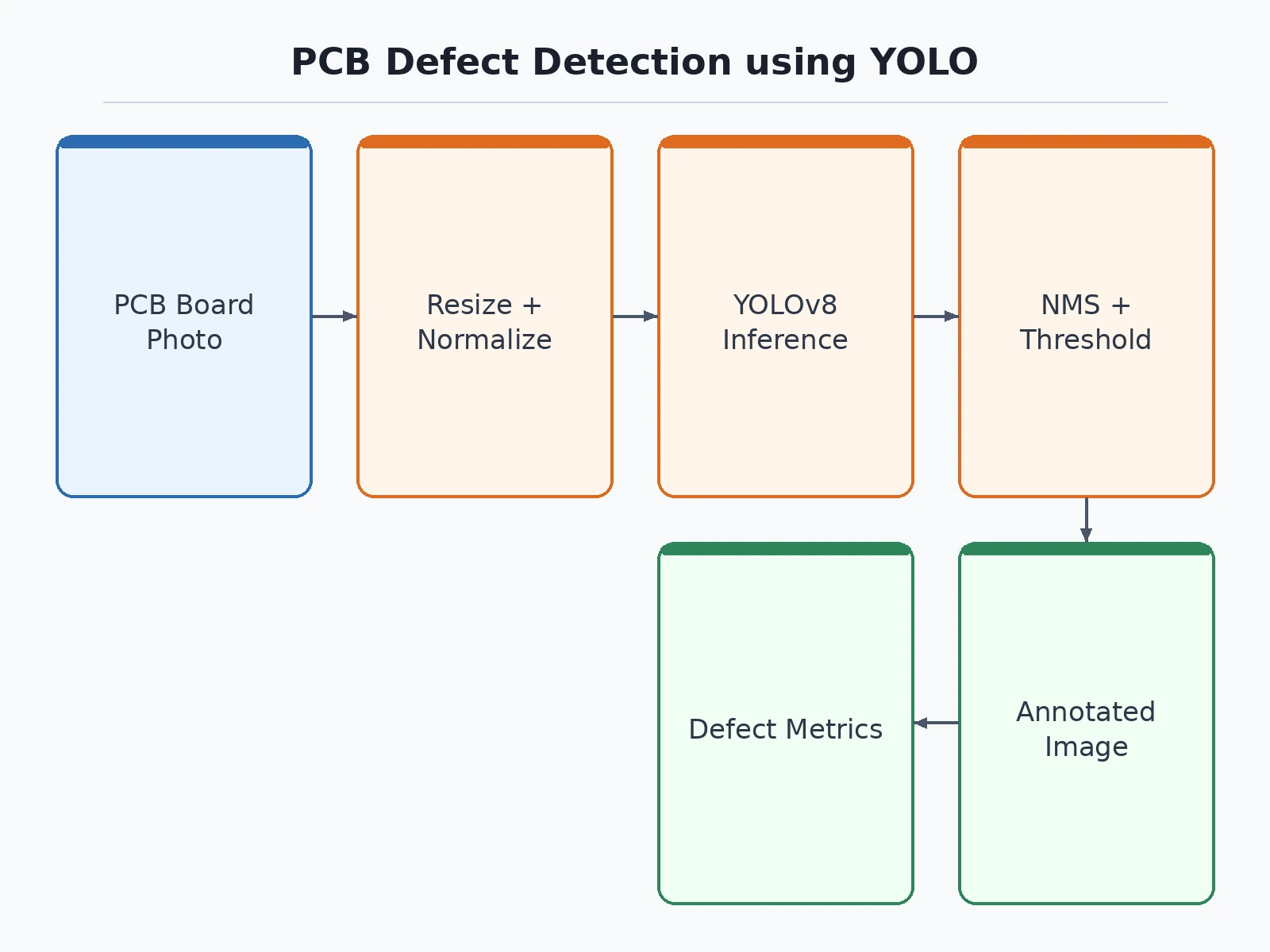
Input: PCB images resized to the YOLO input size.
Prediction: Bounding boxes with defect class and confidence score, in a single pass.
Output: Boxes above an adjustable confidence threshold, with class labels and scores; box-overlaid annotated images.
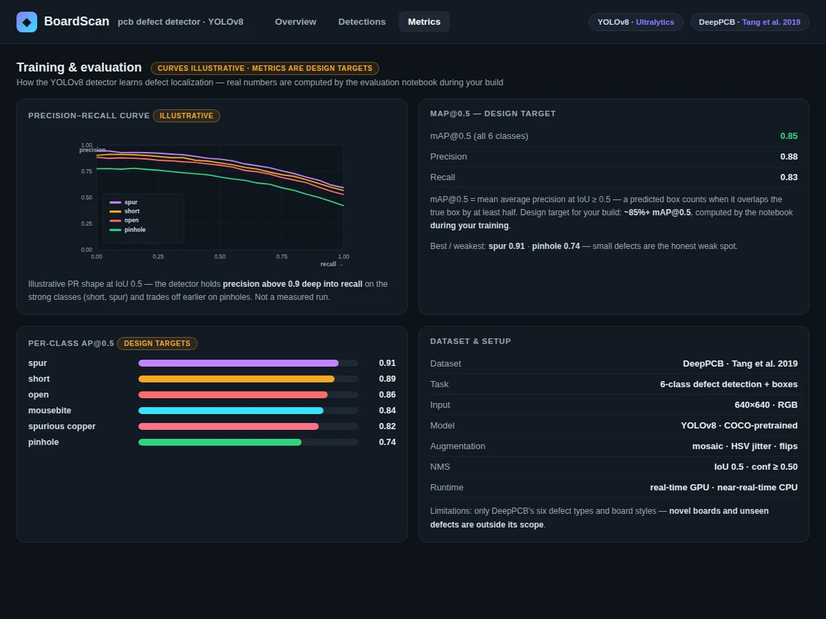
Evaluation metrics: Precision, recall, mAP@0.5 and per-class AP on a held-out validation split — computed by the Jupyter notebook during the buyer's build. No measured performance claimed; design target approximately 85% or better mAP@0.5 on the split.
Working:
- PCB images and defect annotations are loaded from the DeepPCB dataset structure and resized to the YOLO input size.
- Preprocessing: mosaic and HSV augmentation tolerates board lighting and solder-finish variation.
- Training phase: a YOLOv8 detector — pre-trained on COCO and fine-tuned on DeepPCB — trains to predict bounding boxes, defect classes and confidence scores in a single pass.
- Evaluation phase: the Jupyter notebook computes precision, recall, mAP@0.5 and per-class AP on the held-out validation split, with precision-recall curves.
- Inference phase: the trained detector scans new PCB images and outputs boxes above an adjustable confidence threshold; a batch pipeline exports annotated results for a folder of board images.
- Output: bounding boxes with class labels and confidence scores, overlaid on the original images by the visualization script for visual verification.
Specifications:
Model | YOLOv8 single-pass detector (Ultralytics), pre-trained on COCO, fine-tuned on DeepPCB
Dataset | DeepPCB (Tang et al. 2019), public research collection with six defect types
Task | Object detection: bounding-box localization of PCB defects
Classes | Open, short, mousebite, spur, pinhole, spurious copper
Input | PCB images resized to the YOLO input size
Output | Bounding boxes with class labels and confidence scores above an adjustable threshold
Augmentation | Mosaic and HSV, tuned for board lighting and solder-finish variation
Evaluation | Precision, recall, mAP@0.5, per-class AP on held-out validation split — computed during the buyer's build
Design target | Approximately 85% or better mAP@0.5 on the split (target, not a measured claim)
Verification | Box-overlay visualization script for image-by-image checking
Project features
[Six-Defect Box Localization] (implemented) — Bounding-box localization of the six DeepPCB defect types: open, short, mousebite, spur, pinhole, spurious copper.
[Per-Box Labels and Scores] (implemented) — Each box carries a class label and confidence score with an adjustable detection threshold.
[Mosaic and HSV Augmentation] (implemented) — Augmentation pipeline tuned for board lighting and solder-finish variation.
[Per-Class AP Breakdown] (implemented) — Precision-recall curves and per-class AP show exactly which defect types the detector finds hardest.
[Detection Visualization Script] (implemented) — Overlays predicted boxes, labels and scores on PCB images for visual verification of every prediction.
[Batch Inference Pipeline] (implemented) — Exports annotated results for a whole folder of board images.
[Evaluation Notebook] (implemented) — Computes precision, recall, mAP@0.5 and per-class AP on the held-out validation split during the build.
[Instance Segmentation Masks] (future-scope) — Pixel-level defect masks are future work, not included in the base detection build.
What is included
Complete source code (data pipeline, YOLOv8 training, inference and visualization scripts)
Jupyter evaluation notebook (mAP, precision-recall curves, per-class AP, box-overlaid results)
Project report PDF (background, DeepPCB dataset, methodology, evaluation, error analysis)
PPT presentation for final review
Viva Q&A preparation document (YOLO, anchor-free detection, mAP, precision-recall, PCB inspection context)
Setup guide (environment, dataset download, training and inference commands)
Advantages
- Real bounding-box localization of the six DeepPCB defect types — open, short, mousebite, spur, pinhole, spurious copper.
- Per-box class labels and confidence scores with an adjustable detection threshold.
- Per-class AP breakdown plus precision-recall curves show exactly which defect types are hardest.
- Detection visualization script overlays boxes, labels and scores for visual verification of every prediction.
- Batch inference pipeline exports annotated results for a whole folder of board images.
- Evaluation notebook computes precision, recall, mAP@0.5 and per-class AP on the held-out validation split.
Disadvantages
- Only the six defect types and board styles in DeepPCB are known — novel boards, components and unseen defect types will not be detected correctly.
- Small defects against complex copper and silkscreen backgrounds are the hardest cases.
- Design-target-driven prototype on a research dataset — not a production-line inspection system; no line-speed or safety-grade claims.
- Performance depends on the split, augmentation and training conditions of the buyer's own run.
- Board styles, lighting and camera setups far from the training data degrade detection.
Limitations & prerequisites
The detector only knows the six defect types and board styles represented in the DeepPCB data; novel boards, components and unseen defect types will not be detected correctly.
Small defects against complex copper and silkscreen backgrounds are the hardest cases; the per-class AP breakdown documents which types are weakest.
This is a design-target-driven prototype evaluated on a research dataset — it is not a production-line inspection system and no deployed, line-speed or safety-grade performance is claimed.
Performance depends on the split, augmentation and training conditions of the buyer's own run.
Detection quality degrades on board styles, lighting and camera setups far from the training data.
Frequently Asked Questions
Which dataset and model are used?
The public DeepPCB dataset (Tang et al., arXiv:1902.06197, 2019) — board images annotated with bounding boxes for six defect types. The model is YOLOv8 (Ultralytics), pre-trained on COCO and fine-tuned on DeepPCB, with PyTorch as the training backend.
What defects does the detector find?
The six defect types in DeepPCB: open, short, mousebite, spur, pinhole and spurious copper — soldering and etching defects that appear on PCB images.
Is the detection quality guaranteed?
Can this run on a real PCB production line?
No. This is a research-dataset prototype for study and demonstration. A production-line system would need factory-specific labeled data, line-speed cameras and integration work this project does not include.
Is this project suitable for a final-year project?
Yes, for B.E./B.Tech in Computer Science, AI/ML, Electronics and related programs. It demonstrates single-pass object detection, mAP evaluation, per-class error analysis and industrial inspection — strong viva material.
What will I receive, and can it be customized?
Source code (data pipeline, YOLOv8 training, inference and visualization scripts), the evaluation notebook, report, PPT, viva Q&A and a setup guide. Customizable: additional defect types or board datasets, instance-segmentation masks, or an inspection-station interface, scoped at quotation.
Components & software requirements
Python 3.10, Ultralytics YOLOv8 (detection training and inference)
PyTorch (training backend under the Ultralytics framework)
OpenCV (image loading, resizing, box-overlay visualization)
NumPy, pandas (dataset handling, metric computation)
Matplotlib, Seaborn (precision-recall curves, per-class AP plots)
Jupyter Notebook (detection metrics computed during the buyer's build)
DeepPCB dataset (Tang et al. 2019; download guidance in the setup guide)
GPU recommended for YOLOv8 training (cloud-GPU guidance in the setup guide)
Delivery information
Built-to-order: the source code, evaluation notebook, report, PPT and viva kit are prepared fresh for the buyer. Typical delivery spans dataset setup, the YOLOv8 training run, evaluation and documentation; the exact schedule is confirmed at quotation.
Support terms
Setup guidance (environment, DeepPCB download, training and inference commands); viva preparation covering YOLO, anchor-free detection, mAP, precision-recall and the PCB inspection context; customization discussion (new defect types, segmentation masks, inspection-station interface) scoped at quotation.
Download free synopsis (PDF)
Enter your name and WhatsApp number — the synopsis PDF downloads immediately. We may send occasional project updates on WhatsApp; no spam.
Online PCB Defect Detector on a New PCB Defect Dataset (Tang et al., arXiv:1902.06197)