
More project photos (2)
The problem
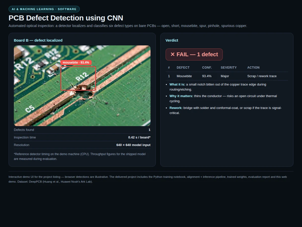
Manual PCB inspection is slow, tiring and inconsistent — inspectors miss hairline opens and tiny solder bridges after hours at the microscope, and small fabrication units cannot afford commercial AOI machines. Automated optical inspection compares each board against a golden reference and flags deviations. The DeepPCB dataset (Huang et al., Huawei Noah's Ark Lab) provides 1,500 template/tested image pairs with bounding-box annotations for six defect classes, mirroring real AOI stations: align, difference, classify. This project implements that pipeline with a modern single-shot detector — template alignment via feature matching, a YOLO-style detection head, non-maximum suppression, and a verdict UI mapping each defect to severity and rework action.
How it works
- The tested board photo is registered to its golden template via ORB feature matching and homography.
- The aligned 640x640 pair feeds a YOLO-style detector with a lightweight backbone (CSPDarknet-tiny/MobileNet).
- The detection head predicts candidate bounding boxes with class scores across the six defect types.
- Non-maximum suppression removes overlapping boxes; survivors below the confidence threshold are dropped.
- Each detection maps to a severity (minor/major/critical) and a rework action for the operator.
- Training uses mosaic + photometric augmentation on the 1,000-pair DeepPCB training split.
Tech stack:
- Python 3.10, PyTorch
- YOLO-style detector (Ultralytics tooling or equivalent)
- DeepPCB dataset (Huawei Noah's Ark Lab)
- OpenCV (alignment, NMS, visualization)
- Flask (demo backend)
- HTML/CSS/JavaScript (demo UI)
- Git
Dataset & Model Details
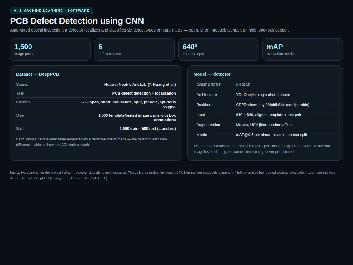
- Dataset: DeepPCB — 1,500 template/tested image pairs with bounding-box annotations, 6 defect classes (open, short, mousebite, spur, pinhole, spurious copper); source: T. Huang et al., Huawei Noah's Ark Lab. Standard split: 1,000 train / 500 test.
- Model input: 640x640 aligned board image. Output: bounding boxes + class + confidence per defect.
- Architecture: YOLO-style single-shot detector; lightweight backbone; NMS post-processing.
- Metric: mAP@0.5 per class and overall, measured on the 500-pair test split after training. No figure is claimed before the training run.
| Parameter | Value |
|---|---|
| Defect classes | 6 (DeepPCB taxonomy) |
| Input | 640x640 aligned board photo |
| Output | Boxes + class + confidence + verdict |
| Alignment | ORB feature matching + homography |
| Inference | Under 1 s per board on CPU (design target) |
| Demo | Board upload + PASS/FAIL verdict |
Project features
- [Six defect classes] Open, short, mousebite, spur, pinhole and spurious copper — the full DeepPCB taxonomy.
- [Bounding-box localization] Every detection ships with a box, class label and confidence, overlaid on the board photo.
- [Template alignment] Tested boards are registered to the golden reference with feature matching before comparison.
- [PASS/FAIL verdict engine] Detections map to severity levels and concrete rework actions (e.g. solder bridge → desoldering wick).
- [YOLO-style detector] Single-shot architecture with a lightweight backbone; 640x640 input, NMS-filtered output.
- [Per-class mAP evaluation] mAP@0.5 measured per class on the 500-pair test split — hardest classes identified honestly.
- [Inspection web demo] Upload a board photo; get boxes, verdict and rework guidance in the browser.
What is included
- Python training notebook (detector training, augmentation, evaluation)
- Template-alignment + inference pipeline code
- Trained detector weights
- Test-split evaluation: per-class mAP@0.5 from the actual run
- Inspection web demo (upload, boxes, severity, rework actions)
- Project report PDF (methodology, error analysis, measured results)
- PPT presentation for final review
- Viva Q&A preparation document
Limitations & prerequisites
- Covers bare-PCB defects only — not assembled-board issues like missing or tombstoned components.
- Needs a roughly top-down, well-lit board photo; extreme angles break the template alignment.
- Tiny defects (pinhole, spur) are the hardest classes — the per-class mAP table shows this honestly.
- Detector training strongly benefits from a GPU; CPU training is very slow.
- Rework actions are guidance for a trained operator, not a repair robot.
Frequently Asked Questions
What is DeepPCB?
A public dataset from Huawei Noah's Ark Lab: 1,500 pairs of defect-free template and defective tested PCB images with bounding-box labels for six defect types — the standard benchmark for PCB defect detection.
Why align to a template first?
Real AOI stations compare against a golden reference. Alignment lets the detector learn the template-vs-tested difference instead of memorizing board layouts, so it generalizes to unseen designs.
Which defects are hardest?
Typically pinhole and spur — they are tiny. The report's per-class mAP@0.5 table identifies the weak classes with measured numbers instead of hiding them.
Can it inspect assembled boards?
No — this project targets bare PCBs. Assembled-PCBA defects are listed as future scope.
Do I need a GPU?
Strongly recommended for detector training. Inference and the demo run on CPU.
Is this project suitable for a final-year project?
Yes — for Electronics, Computer Science and AI/ML programs. It combines object detection, image alignment, industrial evaluation metrics and a genuinely useful inspection demo. Suitable for B.E./B.Tech final-year projects in Electronics, Computer Science and AI/ML.
Components & software requirements
- Python 3.10, PyTorch
- YOLO-style detector (Ultralytics tooling or equivalent)
- DeepPCB dataset (Huawei Noah's Ark Lab)
- OpenCV (alignment, NMS, visualization)
- Flask (demo backend)
- HTML/CSS/JavaScript (demo UI)
- Git
Dataset & Model Details
- Dataset: DeepPCB — 1,500 template/tested image pairs with bounding-box annotations, 6 defect classes (open, short, mousebite, spur, pinhole, spurious copper); source: T. Huang et al., Huawei Noah's Ark Lab. Standard split: 1,000 train / 500 test.
- Model input: 640x640 aligned board image. Output: bounding boxes + class + confidence per defect.
- Architecture: YOLO-style single-shot detector; lightweight backbone; NMS post-processing.
- Metric: mAP@0.5 per class and overall, measured on the 500-pair test split after training. No figure is claimed before the training run.
Delivery information
Built-to-order project. Delivery timeline is shared after order confirmation based on current queue.
Support terms
Complete documentation, setup guide, and viva preparation included. Support for setup and explanation provided.