
More project photos (3)
The problem
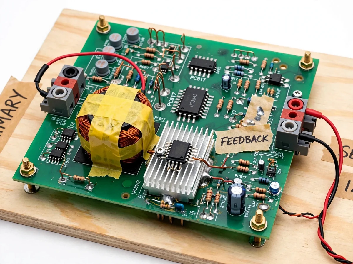
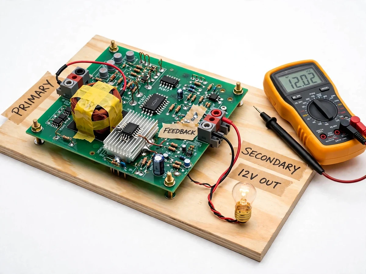
Nearly every electronic device runs on a switch-mode power supply, and the flyback converter is the topology behind countless low-power adapters — yet most students meet it only as a circuit diagram, because commercial adapters are sealed and mains-connected prototypes intimidate beginners. This project makes the flyback tangible and safe: an open-frame demo board powered from a low-voltage DC source (a bench supply or battery) that implements the complete converter — PWM controller, power MOSFET, hand-wound ferrite transformer with primary/secondary clearly separated, output rectification and filtering, and a proper isolated feedback loop using an optocoupler and shunt regulator. Test points expose the switching waveforms, banana-jack terminals give the isolated 12 V output, and a lamp load plus the student's multimeter turn regulation into measured numbers. The board is designed for probing, measuring and understanding — not as a sealed product.
Bench supply or battery feeding the board per the manual.
Follow the working sequence
How it works
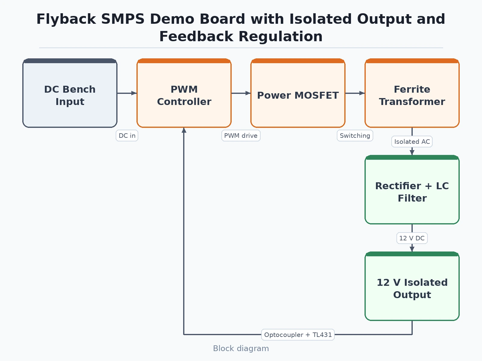
- A DC input (from a bench supply or battery, per the manual) feeds the board; the PWM controller starts switching the MOSFET at its set frequency.
- During each on-time the MOSFET stores energy in the transformer's primary inductance; during off-time that energy transfers to the secondary, is rectified and filtered into the 12 V output.
- The shunt regulator compares a divided sample of the output with its internal reference and drives the optocoupler LED; the optocoupler signals the primary-side controller across the isolation barrier.
- The controller adjusts the switching duty cycle to hold the output at 12 V as the input voltage or load current changes.
- The student measures output voltage at no load and at stepped lamp loads, computing load regulation from their readings.
- The input voltage is varied over the specified range and line regulation is measured the same way.
- Switching waveforms are captured at the test points and annotated in the report against the theoretical flyback waveforms.
Tech stack:
- PWM controller IC (UC3842 class) with oscillator and error amp
- Power MOSFET with aluminium heatsink
- Hand-wound ferrite-core flyback transformer
- Optocoupler (PC817 class) + shunt regulator (TL431 class)
- Output rectifier diode and LC filter
- Banana-jack input/output terminals and test points
- Lamp load set for regulation tests
- Open-frame PCB on insulated base with probe guide
| Parameter | Value |
|---|---|
| Topology | Flyback, discontinuous/continuous boundary (design) |
| Input | DC, approximately 18–36 V from bench supply (design target) |
| Output | 12 V DC isolated, approximately 1–2 A (design target) |
| Switching frequency | Approximately 50–100 kHz (design target) |
| Regulation | Load and line regulation measured by student (procedure) |
| Isolation | Primary–secondary galvanic isolation via transformer + optocoupler (design) |
| Protection | Over-current shutdown, heatsink thermal design (design target) |
| Board | Open-frame demo PCB with marked test points (design target) |
Project features
- [Complete flyback power stage] PWM controller driving a power MOSFET that switches the hand-wound ferrite transformer — the full energy-storage-and-transfer cycle, visible on test points.
- [Hand-wound transformer] The ferrite-core transformer is wound as part of the build documentation, with the turns ratio and the isolation barrier between primary and secondary clearly shown.
- [Isolated feedback loop] An optocoupler plus shunt-regulator (TL431 class) closes the loop across the isolation barrier, holding the 12 V output steady — the key concept of isolated SMPS design.
- [Switching waveform test points] Clearly marked test points let the student observe gate drive, drain voltage and output ripple on an oscilloscope and relate them to the theory.
- [Load and line regulation tests] A lamp load bank and the procedure for stepping the load turn "regulation" into measured percentages in the report.
- [Protection demonstration] Over-current shutdown and thermal behaviour of the MOSFET heatsink are part of the test procedure, not an afterthought.
- [Low-voltage input design] The board runs from a safe DC input (bench supply), so the student experiments freely without mains exposure on the prototype.
What is included
- Complete flyback SMPS demo board (assembled and tested)
- Hand-wound ferrite transformer with winding documentation
- Lamp load set for regulation tests
- Probe guide and test-point map
- Measurement procedure manual (regulation tests, waveform capture)
- Project report PDF (theory, design calculations, readings, analysis)
- PPT presentation for final review
- Viva Q&A preparation document (flyback operation, feedback loop, isolation, DCM/CCM)
Limitations & prerequisites
- The demo runs from a low-voltage DC input for student safety; it is not a mains-input adapter and mains-side design (bridge, bulk cap, EMI filter) is covered in theory only.
- Output power is limited to approximately 12–24 W (design target); it is a teaching converter, not a product power supply.
- Regulation figures are measured by the student on their build — the report presents measured numbers with the test conditions, never a claimed specification.
- The hand-wound transformer's leakage inductance is higher than a commercial part's, which the report discusses as a real design lesson (snubber, ringing).
- Oscilloscope access is assumed for the waveform section; without one, that section uses the provided reference captures with clear labeling.
Frequently Asked Questions
Is it safe for a student to probe?
Yes — the board is designed around a low-voltage DC input, so there is no mains on the prototype; the manual still enforces standard probing discipline.
What does the student actually measure?
Output voltage at stepped loads (load regulation), at varied input (line regulation), ripple, and the switching waveforms at the marked test points.
Why is the transformer hand-wound?
Winding it makes the turns ratio, dot convention and isolation barrier concrete — and its imperfections become the report's most honest section.
How is the output kept at 12 V?
The shunt regulator watches the output and signals through the optocoupler; the controller trims the duty cycle. The loop is drawn, probed and explained in the report.
Can it charge a battery or run a project?
It can power small 12 V loads within its rating, but it is built as a measurement demo board — regulation and waveforms are the deliverable, not a finished adapter.
Is this project suitable for a final-year project?
Yes — for Electrical and Electronics programs. It is a real switching converter with magnetics, feedback and measured regulation. Suitable for B.E./B.Tech final-year projects in Electrical and Electronics Engineering.
Components & software requirements
- PWM controller IC (UC3842 class) with oscillator and error amp
- Power MOSFET with aluminium heatsink
- Hand-wound ferrite-core flyback transformer
- Optocoupler (PC817 class) + shunt regulator (TL431 class)
- Output rectifier diode and LC filter
- Banana-jack input/output terminals and test points
- Lamp load set for regulation tests
- Open-frame PCB on insulated base with probe guide
Delivery information
Built-to-order project. Delivery timeline is shared after order confirmation based on current queue.
Support terms
Complete documentation, setup guide, and viva preparation included. Support for setup and explanation provided.
Download free synopsis (PDF)
Enter your name and WhatsApp number — the synopsis PDF downloads immediately. We may send occasional project updates on WhatsApp; no spam.