
More project photos (2)
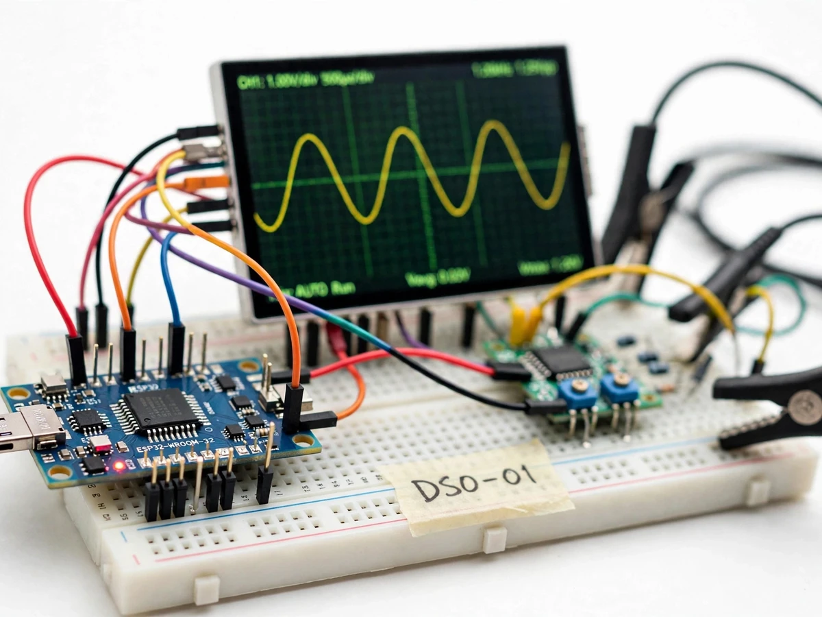
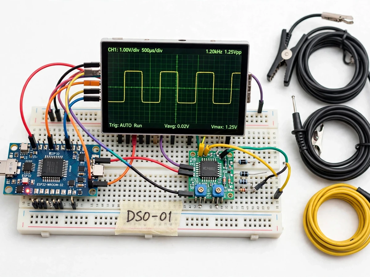
The problem
Every electronics lab has an oscilloscope, but few students ever understand what is inside one. A digital storage oscilloscope is the perfect capstone for an Electronics or E&TC final-year student: it forces you to connect analog design (the front-end must condition a ±20 V signal down to the ADC's 0–3.3 V window without loading the source), embedded programming (high-speed ADC sampling, DMA double buffering, real-time rendering), and signal processing (trigger detection, RMS/Vpp/frequency computation) in one working instrument. Commercial bench scopes cost tens of thousands of rupees; this project proves the same core ideas — sampling, triggering, measurement, display — can be built around a sub-₹500 microcontroller. The student ends up with a genuine test instrument on the bench, plus the rare ability to explain every block in the viva: why the front-end attenuates before amplifying, why a 1 MSPS sample rate caps usable bandwidth near 20 kHz, and how a rising-edge trigger actually finds the trigger point.
1x/10x compensated passive probe feeding the input attenuator.
Follow the working sequence
How it works
- The input signal passes through a 1×/10× selectable attenuator and clamping-diode protection, then an op-amp stage scales and level-shifts it into the ESP32 ADC's 0–3.3 V window.
- The ESP32 ADC samples the conditioned signal at the design-target rate (up to 1 MSPS combined across both channels) into DMA double buffers so sampling never pauses during rendering.
- Firmware scans the incoming buffer for the trigger event — rising or falling edge crossing the touch-set trigger level — and aligns the displayed window on that point.
- The 320×240 TFT redraws the trace on a 10×8 grid with gridlines, channel colors, trigger marker and the auto-computed measurements on each sweep.
- Touch controls adjust timebase (seconds/div), volts/div per channel, coupling, trigger level, run/stop and single-shot; settings persist in flash.
- Pressing capture stores the current buffer in flash as a named snapshot; recalled snapshots render exactly like live traces for comparison.
- Measurements (Vpp, RMS, DC offset, frequency) are computed from the triggered buffer each sweep and updated on screen.
Tech stack:
- ESP32 (dual-core Xtensa, Wi-Fi/Bluetooth)
- ESP32 12-bit SAR ADC with DMA sampling
- 2.8-inch SPI TFT touchscreen (320×240)
- Op-amp analog front-end with 1×/10× attenuation
- ESP-IDF / Arduino-ESP32 firmware (C++)
- FreeRTOS task scheduling
- KiCad schematic and PCB layout
- Passive oscilloscope probes (1×/10× compensated)
| Parameter | Value |
|---|---|
| Channels | 2 (simultaneous) |
| Sample rate | Up to 1 MSPS combined (design target) |
| ADC resolution | 12-bit SAR (ESP32 on-chip) |
| Usable bandwidth | Approximately 20 kHz (design target) |
| Input voltage range | ±20 V (with 10× attenuation); ±2 V (1× range) — design targets |
| Timebase range | 10 µs/div to 2 s/div (design target) |
| Display | 2.8-inch TFT, 320 × 240, SPI with resistive touch |
| Trigger modes | Auto, Normal (rising/falling edge), Single-shot |
| Measurements | Vpp, RMS, DC offset, frequency (computed per sweep) |
| Snapshots | 8 stored traces in flash |
Project features
- [Real 2-channel acquisition] Dual-channel sampling through the ESP32's 12-bit SAR ADC with DMA double buffering (design target 1 MSPS combined), so a waveform and a reference trace are captured simultaneously.
- [Analog front-end with protection] Op-amp based input stage with selectable attenuation (1×/10×), DC level shifting into the ADC window, and clamping-diode overvoltage protection rated for the 0–3.3 V input range.
- [2.8-inch TFT touchscreen UI] 320×240 SPI TFT rendering the live trace on a grid, with touch buttons for timebase, volts/div, coupling, trigger level and run/stop — the whole instrument runs on the device.
- [Edge + auto trigger modes] Rising-edge, falling-edge, auto and single-shot triggering implemented in firmware, with a visible trigger-level marker and a trigger-position indicator on screen.
- [On-screen measurements] Automatic Vpp, DC offset, RMS and frequency readouts computed from the captured buffer, plus cursors that can be dragged by touch.
- [Waveform snapshot capture] Store up to 8 captured traces in flash and recall them later for comparison — demonstrated in the viva without a live signal.
- [Buyer-run calibration procedure] A step-by-step guide using a known reference source: measure a documented test signal, adjust the front-end gain trim, and verify the readout accuracy yourself.
- [Probe set included] Two passive probes with grabber clips built around compensated divider tips, wired and tested for the 1×/10× front-end ranges.
What is included
- Assembled ESP32 DSO unit with 2.8-inch TFT touchscreen, analog front-end and enclosure
- Two passive probes with grabber clips
- Complete firmware source (ESP-IDF / Arduino-ESP32, FreeRTOS-based)
- Analog front-end schematic, KiCad PCB layout and bill of materials
- Buyer-run calibration procedure with reference test signals
- Project report PDF (background, sampling theory, front-end design, firmware architecture, calibration results procedure)
- PPT presentation for final review
- Viva Q&A preparation document (Nyquist, ADC quantization, triggering, op-amp conditioning, aliasing)
Limitations & prerequisites
- Usable bandwidth is approximately 20 kHz — this is a teaching/bench-aid instrument, not a replacement for a bench scope on high-frequency circuits.
- ESP32 ADC non-linearity is well documented (especially near 0 V and 3.3 V); the firmware applies a lookup-table linearization, and residual error is quantified in the buyer-run calibration — never claimed as a factory measurement.
- Maximum 1 MSPS combined across two channels; both channels on halves the per-channel rate.
- The input range is a design target verified against the reference procedure — sustained input beyond ±20 V (10× range) can damage the front-end.
- TFT refresh caps the rendered sweep rate; very fast bursts render as aliased envelopes exactly like real DSOs, which is itself a teaching point on aliasing.
- Requires a stable 5 V / 1 A supply; brownouts corrupt the ADC reading and the firmware flags supply sag on screen.
Frequently Asked Questions
How fast can this oscilloscope sample?
The design target is up to 1 MSPS combined across both channels using the ESP32's ADC with DMA double buffering. That gives a usable bandwidth of roughly 20 kHz — honest, quantified, and enough to view audio, sensor, PWM and motor-drive signals.
Is the TFT display touch-controlled?
Yes — the 2.8-inch 320×240 SPI TFT is a touchscreen. Timebase, volts/div, coupling, trigger level, run/stop and capture are all driven by on-screen touch buttons; there is no separate computer or app.
How accurate are the measurements?
Voltage and frequency readouts are computed from the captured buffer and verified with the buyer-run calibration procedure against a reference source. No accuracy is claimed as measured before that procedure is run on the actual built unit.
What can I use as test signals?
The calibration guide uses signals you already have: an Arduino or 555-timer square wave, a function-generator app tone through a small speaker driver, and a PWM output from any dev board.
Can it capture a single event?
Yes — single-shot trigger mode captures the first rising or falling edge after the trigger level is armed, and the snapshot can be stored in flash and recalled later.
Is this project suitable for a final-year project?
Yes — for Electronics, E&TC, Electrical and IoT & Embedded programs. It demonstrates analog front-end design, embedded firmware with DMA, signal-processing fundamentals and instrument UI design. Suitable for B.E./B.Tech final-year projects in Electronics, E&TC, Electrical and IoT & Embedded.
Components & software requirements
- ESP32 (dual-core Xtensa, Wi-Fi/Bluetooth)
- ESP32 12-bit SAR ADC with DMA sampling
- 2.8-inch SPI TFT touchscreen (320×240)
- Op-amp analog front-end with 1×/10× attenuation
- ESP-IDF / Arduino-ESP32 firmware (C++)
- FreeRTOS task scheduling
- KiCad schematic and PCB layout
- Passive oscilloscope probes (1×/10× compensated)
Delivery information
Built-to-order project. Delivery timeline is shared after order confirmation based on current queue.
Support terms
Complete documentation, setup guide, and viva preparation included. Support for setup and explanation provided.
Download free synopsis (PDF)
Enter your name and email — the synopsis PDF downloads immediately. We may send occasional project updates; no spam, unsubscribe anytime.